Guido Araujo
SePtember
2002
brazil IP
NETWORK
The time
has come….
I THE brazil IP network
BRAZIL IP
is an initiative to organize Brazilian academic and R&D institutions around
a collaborative and distributed network capable of delivering Virtual Socket
Interface (VSI) or Motorola SRS compliant Intellectual Property (IP)
semiconductor cores.
The
mission of such network is twofold. In the short run, it aims at increasing the
country expertise in designing world-class integrated circuits, by exposing the
participating institutions to real-world design practices and evaluation. In
the long run, Brazil IP seeks to create the conditions for the establishment,
in the country, of local Design Houses (DHs) capable of competing in the
international IP market.
The
Brazil IP effort is inspired in previous successful network experiences in
Brazil and abroad (http://www.design-reuse.com), and in
the belief that a sustainable long term growth in this area will only be
possible through the generation of enough design experience critical mass. This
initiative is based on three central ideas: (a) world-class design standards;
(b) solid financial support; (c) stringent design evaluation. It is organized
around an IP repository (http://www.brazilip.org) and a
service design center.
This
document defines the basic premises for the creation and evolution of the
Brazil IP Network. It does not cover the details and technical issues required
for its final implementation. It is not intended to be a final project.
On the contrary, it was put on public domain to be criticized and thoroughly
scrutinized by all players in the area, in the hope that it can contribute to
its consolidation. Its goal is to contribute to the debate that has been
undergoing under the coordination of MCT, and as such, it is complementary to
that effort.
This
document is divided as follows. Section II makes a thorough analysis of the
international IP market tendencies. It is based on over 30 papers and reports
from market research firms, and it has for goal to identify the best insertion
strategies for potential Brazilian DHs. Section III is an overview of the Brazilian
Microelectronics Plan (PNM), an initiative of the Brazilian Ministry of Science
and Technology to organize and fund the activities in this area. This section
also discusses the main challenges faced by such program. Section IV analyzes
the role of the academia in the microelectronics field and suggests how it
could contribute to the Brazil IP effort. Sections V, VI and VII respectively
describe the three central mechanisms for the implementation of such network,
namely The Brazil IP Challenge, Center and Repository. Section VIII wraps-up
with final conclusions and suggestions for future line of actions.
II THE international
Ip MARKET
The 90’s
have witnessed an explosive growth in the demand of electronic products to
attend the infrastructure of the Internet and telecom networks. The competitive
and high volume nature of these markets has considerably impacted the way electronic vendors design and sell their
products. The immediate consequence of
that was a very fast reduction in new products time-to-market, and an
increasing pressure for design cost reduction. This scenario created new
demands for the electronic system designers, which had to struggle to keep up
with very tight schedules and stringent design constraints. The design cycles for new products shrank
from two years in 1990 to 6 months nowadays. As a result designers started to
put together a number of pre-verified modules into the same die, thus meeting company demands for fast and cheap
designs. Reusing in-house modules soon became a central methodology for
semiconductor vendors.
On the
other hand, the improvement in VLSI technology density
enabled designers to integrate very
complex circuits into a single die. The availability of sophisticated VLSI technology came at the
expenses of a tremendous increase in
the capital requirements to build and operate a fabrication plant. The very
high operational costs of a semiconductor company has been responsible for a gradual desegregation of that industry
[10]. The semiconductor business has been transitioning from a vertically
integrated structure, in which a single company performed the entire
semiconductor process, from design to manufacturing, to a horizontal model in
which companies focus on their core
business been it equipment, circuit
manufacturing, design integration, design automation or more recently,
intellectual property. Semiconductor equipment companies, like Applied
Materials, were the first to separate from the vertically integrated industry.
This was followed by the rise of foundries and companies, such as TSMC
and UMC, which focused exclusively on manufacturing [10]. The emergence of
silicon foundries, offering manufacturing services, closed the final scene in the desegregation of the semiconductor
industry. New fabless semiconductor companies, or IP (Intellectual
Property) providers emerged offering
high-value pre-validated modules (known as IPs) direct to end customers.
These companies license IP cores to those with the expertise and capacity to
produce the silicon.
A
high-quality IP can often help to achieve a significant reduction in
time-to-market for a new product. A second key factor determining the value of
an IP is the number of times that it can be reused, spreading the value over
multiple projects. The highest value IP has a long life, being reused in a
great variety of projects. The first
modules in the IP market reflected that need of long term reusability. In fact
the first IP company, ARM Holdings PLC, delivered in 1990 the ARM
microprocessor which has since holding
the largest share of the IP market.
Even nowadays, the IP market is still dominated by companies that
provide “best of the class”, highly reusable modules like microprocessors (e.g.
MIPS Technologies), buses (e.g. Rambus Inc.) and memories (e.g. Virage Logic).
AN
OVERVIEW OF THE IP MARKET
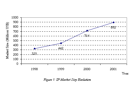
According
to Dataquest [3] the IP market has grown at very high rates,
around 46% a year . The graph of Figure 1 tracks this evolution since 1998.
Interesting enough, despite the very bad business conditions in 2001, the IP
market grew 25%, totaling US$ 892 million, an impressive number given that the
semiconductor sector had a 31% decrease in revenue.
Dataquest
forecasts a compound annual growth of 35% for this market over the next 4
years. According to Cahners In-Stat Group, a high-tech market research firm
that accompanies the IP market, independent IP provider revenues should top US$
1.6 Billion by 2005 [3].
The
composition of the IP market, with respect to the industry sector it operates,
is clearly defined. The communications sector dominates and will continue to
dominate IP licensing over the next several years [22] with a market share of
about 57%. The majority of communications IP licensing revenue comes from high complexity designs to
support telecom infrastructure requirements. The second largest end-user market
is the consumer electronics.
The IP
business is still predominately dominated by the high-value, easy to verify
modules [29]. Microprocessor blocks dominate worldwide IP revenue, reaching US$
292 Million (33%) of the market in
2001. Bus interface blocks such as PCI, USB and IEEE 1394 have proven to be
popular functions for third-party IP providers because of the easy of
verifying. Bus interface is the second largest category, reaching US$ 140
million (17%) in 2001.
The IP
market business models are organized around three acquisition practices (sale,
licensing, and royalty). Of the three models, licensing accounted for about
61%, royalties 22% and services/sale 17% of all revenues in 2000. According to
Cahners In-Stat [22], licensing share of the business models should reach
nearly 95% by 2005.
Although
there are approximately 450 IP vendors tracked by Gartner Dataquest, only a few
players have been able to build a successful business by offering customers
standalone silicon IP blocks [33]. The distribution of the top 10 semiconductor
IP vendors by Revenue (Millions of US dollars) during the year of 2001 is shown
below in Table 1.
Successful
companies like the top three vendors, ARM, Rambus and MIPS Technology continue
to dominate the market (40% of the total), although the three leaders as a
group lost share compared to the smaller vendors. This concentration has been
unchanged for a number of years now, reflecting a certain immaturity of such
market. The reasons have probably to do with the lack of standards for the
design and delivery of IPs as commodities. Although initiatives like the
Virtual Socket Interface (VSI) Alliance are underway, small vendors still
cannot rely on such standards to prove the quality of their IPs to the market,
as opposed to well-known companies that can count with strong marketing and
networking strategies.
|
Company |
2001 market share (%) |
2000 market share (%) |
2000-2201 GROWTH (%) |
|
ARM |
20.1 |
18.2 |
37.6 |
|
RAMBUS |
12.0 |
13.3 |
12.8 |
|
MIPS
Technologies |
7.9 |
12.4 |
-20.7 |
|
Synopsys |
5.0 |
4.7 |
33.0 |
|
TTP
Com. |
3.9 |
3.4 |
44.9 |
|
Virage
Logic. |
3.9 |
3.2 |
52.9 |
|
Mentor
Graphics |
3.4 |
4.8 |
10.5 |
|
Parthus
Technologies |
3.4 |
2.3 |
86.8 |
|
Artisan
|
3.1 |
2.9 |
33.6 |
|
DSP
Group |
3.0 |
3.5 |
6.0 |
|
Others |
34.3 |
31.3 |
37.0 |
|
Total
Market |
100.0 |
100.0 |
25.0 |
Table 1: IP vendor market share distribution [1]
IP
BUSINESS TENDENCIES
In order
to better understand the tendencies in this market it is important to
categorize the IP business. In this text we will use the IP market segmentation
model by Eric Chen from J.P. Morgan H&Q [15]. The basis for this
classification is that IP is considered a business model rather than an
industry.
In
Chen’s view, IP is an information
product and as so its reproduction cost approaches zero, thus leaving very few
opportunities for late market entrants, unless they can associate a very high value to its product. In this
case, commodity IPs, like those that could be easily created by a system
house own engineers or by other IP vendors, are doomed to failure. In Chen’s
second category are the environmental IPs. These are IPs that address
huge and urgent problems that are common to a large number of system vendors.
It is a risky business, given that it
requires the entire industry to co-invest with the company, but that also can
create value to those IP vendors that succeed, because of the barriers that it
imposes to potential competition. Chen’s, third category, product IP,
addresses a more familiar design reuse market. They are formed by companies
that offer high-valued “best of the class” IPs like ARM and MIPS. Domain IP is Chen’s last category,
and is formed by a set of IP modules put together as a platform IP for an
application specific solution in a particular domain.
The IP
business is still undergoing its infancy, and
a number of new players and business models are coming into picture.
During last year three important shifts have been observed in the IP market:
(a) an increase in the number of semiconductor OEMs that are licensing their
IPs; (b) the consolidation of the platform IP as a relevant market segment; and
(c) the emergency of software IPs vendors. Below we analyze each one of those
tendencies under Chen’s IP categorization.
Commodity
IP vendors are starting to find tough competition from traditional
semiconductor companies working as
OEMs. For example, Fujitsu started to trade its communication-centric blocks
last April in the Virtual Component Exchange, an IP on-line catalog. If this
becomes a real tendency, it can make it
even more difficult for small IP vendors to enter the market without a
high-valued module.
An
important direction which clearly seems to take form is the interest in
platform IP technology (or domain IPs in Chen’s classification). Companies like
Parthus Technologies plc [27] and Tality [21] are promising platform IP provider. Parthus has established itself as
a leading player in the silicon IP market by offering platforms along with
design services. The company takes both third-party cores, such as the ARM7
processor, and its own IPs and wraps them together, in base platforms, for
applications like wireless terminals and Bluetooth peripherals. Parthus IP
market share grew 86% during 2000-2001
[27].
As many
vendors started to include protocol stacks, drivers and other software routines
for their increasingly application-specific functions, software licensing
associated with semiconductor IP is transforming the market. License software has more than doubled in
2001, going from about US$ 30 million in 2000 to US$ 65 million in 2001.
According Jim Tully, Chief analyst of Gartner Dataquest Group [19] software IP
is forecast to grow at well above the hardware IP rate over the next few years,
although it is probably the conjunction of hardware and software IP, together
with the appropriate design service, that will be the most winning strategy.
In
general, the current tendencies of the IP market point to an increase in the
demand of complete IP solutions. This seems to favor, in the long run, a market
dominated by platform IPs, containing a number of semiconductor and software IPs working together to address a
particular class of applications. It is still not clear if the individual IP
components of such platform will come from the traditional semiconductor
vendors (as OEM parts), commodity IP vendors or developed by the platform IP
vendor itself. The most probable
picture is that it will be composed of a mix of those, with the largest share
of the basic commodity IPs coming from the OEM market. If such a picture
becomes reality we will see a very high entry barrier for new commodity IP
providers.
The current tendencies of the IP market point
to an increase in the demand of complete IP solutions. Thus, any new IP provider entrant,
particularly small Brazilian DHs,
should concentrate its effort in designing cores that: (a) provide a
high-valued solution for some specific niche; (b) could eventually contribute
to assemble a relevant platform IP.
III THE BRAZILIAN MICROELECTRONICS
Plan
In this
section we analyze the central goals of the Brazilian National Microelectronics
Plan (PNM), an effort from the Brazilian Ministry of Science and Technology
(MCT) to organize the R&D and
business activities in the country. The central goal of PNM is to create the
conditions for the development of
microelectronics business opportunities in Brazil.
The main
motivation behind PNM is the increasing weight of semiconductor components in
the Brazilian trade balance deficit. According to Scartezini [20], Secretary
for Information Technology Policy of MCT, semiconductor imports are the second contributor to Brazil trade deficit, corresponding to
US$ 1.2 Billion in 2000 (US$ 1.8 Billion in 2001). In order to revert this
tendency, MCT proposed, through PNM, the following strategic line of action
[20], that forms the basis for the country long term microelectronics policy:
·
The
focus of the policy should be on R&D and marketing of IP cores
·
Improve
the R&D and Human Resources (HR) infrastructures
·
Create
opportunities for innovation in the electronic industry
·
Develop
work on the legal and economic sides of microelectronics business
·
Work
toward Congress approval of the IC Act
For the purpose of the analysis of the relation of PNM and Brazil IP
this document will consider only the first two items above. All other items
have been extensively discussed by Scartezini [20], Franca-Neto [24], Machado
[35] and others during the Workshop on The Global Integrated Circuit Design
Market, held by MCT at the Genius Institute, November 5th, 2001 in
Manaus, Brazil (http://www.genius.org.br/PNMICRO/index.htm).
In order to enable the development of an IP industry in Brazil, the PNM
business plan [20] propose: (a) to increase the funding of IC design initiatives;
(b) to build a basic prototype facility that can be used for design validation;
(c) to work towards attracting people to design activities; (d) to fund the
conditions for the establishment of Brazilian DHs. These tasks are thoroughly
discussed bellow.
·
Funding
IC design initiatives.
From the MCT perspective [20], the funding for the microelectronics activities
in Brazil would come from the so called sector funds, a number of
financial mechanisms, backed by Brazilian Federal Government taxes collected
from certain sectors of business (e.g. telecom and computer industries).
·
Building
a prototype foundry.
A large effort has been put in place, with the help of Motorola Semiconductor
to set up a 0.35 micron CMOS semiconductor plant in Porto Alegre (RS). A group
of researchers from the Federal University of Rio Grande do Sul (UFRGS) is
working to put together this facility. After it is complete, this plant should
permit designers from R&D centers
and small DH in Brazil to prototype and validate their own chips, without
having to incur in large NRE[2]
costs and to wait for long turn around times at other foundries abroad.
·
Attracting
HR to the design area. One of the central activities proposed by
the PNM document is to train students from various areas like EE and CS in IC
design techniques. To achieve that, it anticipates the establishment of a few
Training Centers located in places like Campinas (SP), São Paulo (SP) and Porto
Alegre (RS). Two types of centers will be created: Professional and Teaching
Centers. A Professional Education Center was established at the Eldorado
Institute, a center with close ties with the Brazilian Semiconductor Technology
Center (BSTC), a Motorola DH located in Jaguariúna (SP). The idea behind that
is to leverage on the BSTC expertise to offer world-class training programs for
potential DH designers. Teachers Formation Centers are co-located at LSI/USP,
CCS/UNICAMP and CEITEC/UFRGS, and will work as training centers for university
professors on various microelectronic technologies.
·
DH
funding mechanisms.
The last, and possibly the most important activity proposed by the PNM document
is the creation of the conditions for the establishment of local DHs in Brazil.
PNM addresses this by the creation of a few DH incubators in places like Manaus
(AM), São Paulo (SP) and Florianópolis (SC). These DH would receive a
tremendous financial support and a very good business environment that can back
their operation for the time required to achieve adequate insertion into the
international IP market. As suggested by Franca-Neto [24] such a DH should have
around 50 people, and an initial financial support close to a couple million
dollars to design an 80K digital circuit in two years.
THE
CHALLENGES
The ideas
proposed at the PNM document seem very coherent with the country reality and
the need to push this industry. The players involved in the process are clearly
identifiable: MCT, Genius Institute, Eldorado Institute, CPqD, CEITEC, Fundação
CERTI, etc…, various university groups across the country, and state
governments. Companies like Motorola have been providing a strong support to
this effort.
From the
financial side the long term perspectives of PNM will depend on how effectively
microelectronics is perceived as a relevant area in Brazil’s Science and
Technology long term strategic plan. Comments from the political arena have
been recently supporting that, mainly due to a perception that the absence of
this technology can considerably impact, not only the country’s trade balance,
but also its ability of improving competitiveness in the global market.
One of
the goals of the PNM project is to create conditions for the establishment of
Brazilian DHs. Two basic conditions are described in the PNM document that are
said to create the opportunities for that: (a) Existence of funding mechanisms;
(b) Availability of trained HR. We analyze each one of those below.
Existence
of funding mechanisms.
Assuming that a political consensus is formed around the need to finance IC
design in the country, we believe that enough resources from the sector funds
will be available to do that. At the cost of a couple million dollars to
finance each one of the first DHs, the task of deciding which IP to design
becomes crucial. Two factors make this decision central to the success of any
new DH. First, as discussed in Section II, commodity IPs are starting to play a
diminishing role in the IP market, giving the increase in the number of
offerings of semiconductor vendors own IPs as OEM parts, and the clear long
term tendency toward platform IPs. In order to succeed in the commodity IP
market the DH will have to practice a dumping license policy, combined with a
roadmap of gradual increase in license fees. This will imply in heavy subsidies
to finance the DH operation in the long run.
An alternative to that is for the DH to target a high-valued IP, which
attends a specific demand of some market niche. This goes in the same direction
as the suggestion by Franca-Neto [24] when he says that the DH “should go for
the gold”. But it is not easy without the help of IP market experts and a
strong foundry partnership. The PNM has adequately anticipated that and
assigned capital resources to hire consultants to do the job.
Availability
of Trained HR. As
suggested by Franca-Neto [20], a DH
would require around 50 trained professionals to deliver an 80K gate IC in two
years. It is expected that to deliver such a design the DH will need to hire at
least a few experienced IC designers to form the core of the DH. Unfortunately,
almost all such experts already work for centers like BSTC, left the country
seeking a better job opportunity, or simply switched to another area. From the
PNM document it is expected that a large number of professionals will be formed
by the Professional Training Centers to attend this demand. Nevertheless, one
has to notice that the professionals formed by these centers will be recently
graduated EE/CS students, lacking enough experience to join a million dollar
start-up that has for goal to design a real-world IP core. Moreover, these
professionals will be highly disputed by DHs like BSTC or other international
DHs considering installing in the country. Therefore, a situation has been
reached, in which to create a local DH one needs at least a few experienced
designers, but to have these designers one has to train them, and to keep
training (and paying) them until they have enough expertise to handle designs
that are complex and competitive enough for the international market. The
Brazil IP effort aims exactly at increasing the number of opportunities for
these designers to work on real-world projects. Without that, it is our opinion
that it will be very hard to keep enough design critical mass in the country to
enable the establishment of local DH. A
complementary alternative is to make it
attractive for international DHs to come to the country, while waiting that
eventually a small set of engineers will spin off such companies to build their
own DHs. Although effective in the long run, there is no guarantee that such
spin-offs would eventually occur.
The creation of new financing mechanisms like
the sector funds will give Brazil enough capital to support a few local DHs.
Nevertheless, the country does not have enough experienced designers to
leverage on that. The HR critical
mass is scattered and urgently needs to
be networked and organized around international design standards and
evaluation. In other words, the country has the capital but not enough people
to do the job.
iV THE academia: RAising standards
During
the late 80’s, Brazil had a reasonable number of microelectronics groups
working in universities, R&D and industry centers. Many of those groups
have been formed during the days of the so-called “Reserva de Informática” (RI), a set of industrial policies aimed
at strengthening the country’s computer
industry. It is not the purpose of this document to evaluate what went wrong in
that strategy, but on the other hand, it is very relevant to analyze its impact in the current state of
the area.
The RI policies were organized as a vertical
framework in which every sector of the computer industry was protected from
foreign competition by import barriers. One of the sectors which benefited most
from those policies was microelectronics. The microelectronics industry was
strongly subsidized, as well as R&D centers and universities. Moreover,
people in the microelectronics academia community those days, together with the
local industry, had an important role in defining the country policies for that
sector. Unfortunately, those policies were strongly based on a xenophobic view
of the world, in which foreign partnership was considered out of question.
Eventually, a combination of bad
planning and poor delivery undermined the whole RI strategy. After 20 years the
results of that policies are still echoing. The microelectronics R&D
activities have been ignored during all these years, while the whole area has
been tagged as unable to deliver.
The
results of that had a strong impact in the development of microelectronics in
the country. Many promising researchers and designers drop off the area and/or
left the country, while those who continued working in it had serious problems
in attracting good people and financing their work. Even worse, the
self-confidence of a whole new generation of researchers and designers was
destroyed, leading them to believe that they could only play a minor whole in
Brazil’s R&D effort. As a result, people in the area concentrated their
efforts in teaching and maintaining what remained of their labs and personnel,
in an arduous fight for survival. Efforts to improve standards were immediately
abandoned by the lack of self-confidence and/or lack of credibility by the
funding agencies. As a member of that community put it (E.J.P. Santos) “in this
country basic sciences get much more funding than microelectronics”, an amazing
distortion for a country that urgently needs industrial innovation. Santos and
others favor policies that promote a shift in the country’s C&T paradigm toward supporting basic and
applied research as well.
The main
result of that is a deep trust gap between academia, funding agencies and
industry. From the industry perspective the academia is not capable of
developing world-class R&D activities, while from the academia point of
view, the industry only interest is to cash in a couple of dollars through its
foundations. Both are wrong. It is
extremely important that this mistrust be urgently eliminated. As reminded by
Franca-Neto, in his PNM talk [24], it was precisely the synergy between
universities and companies that made the Silicon Valley what it is today. In
countries like Brazil, which desperately needs to improve its productivity,
this lack of confidence is not only unfortunate but also deadly. One of the
goals of the Brazil IP effort is to agglutinate the best of academia and
industry into a mutually beneficial project. To achieve that, both parties need
to seat and to collaborate much more intensively than today, especially given
that the level of microelectronics activities
outside the academia or centers like BSTC, Eldorado, Genius and others is very
small.
On the other hand, the academia has to make an effort to organize itself
around common long-term goals. The current situation in such community, in
which separate groups make individual efforts aiming at their own local agenda,
does not help anyone. On the contrary, it only benefits the maintenance of the
current situation of lack of confidence and poor results.
It is very important that the microelectronics
academia increase its efforts to demonstrate that: (a) it can participate in collaborative
projects; (b) it is capable of
delivering world-class R&D activities; (c) It is capable of dealing with
world-class standards and evaluation.
v THE brazil IP network
Brazil IP is an attempt to organize the
microelectronic design groups in Brazil around a collaborative network of
design centers capable of delivering Virtual Socket Interface (VSI) or Motorola
SRS complaint Intellectual Property (IP) semiconductor cores. The mission of this network is twofold. In
the short run, it aims at increasing
the country expertise in designing world-class integrated circuits, by exposing
the participating centers to real-world design practices and real-world
evaluation. In the long run, Brazil IP
seeks to enable the conditions
for the establishment, in the country of local Design Houses (DHs) capable of
competing in the international IP market.
THE ONSA NETWORK: A SUCCESFUL
EXPERIMENT
Brazil IP central idea leverages on the success
of a similar effort, known as the ONSA Network, which formed the core of
the Genome Project, an initiative
financed by FAPESP, the State of São Paulo R&D agency. The ONSA network
guided the work of a number of laboratories toward a single goal: sequencing
the genome of a pathogen commonly found in orange plantations. Other genomes
have been successfully sequenced since then. It is important to understand what
made ONSA a worldwide success.
·
Task
Distribution. First
of all, the work was divided among a large number of Biology laboratories
(around 50) which produced independent genome pieces (sequence of nucleotides)
that were assembled together by a central bio-informatics laboratory. This
considerably sped-up the project results, while maintained laboratories working
under their won administration and operation mode. Moreover, given that no
laboratories (but the central laboratory)
was in charge of a specific part of the project, if a lab was not
capable of delivering results for some reason, another lab would eventually
produce the missing part. In order to participate in the network each lab
received an initial package containing sequencing machines and the required
materials.
·
Payment
Based on Performance.
The communication of each lab with the central lab is performed through the
Internet. After a genome piece is sequenced by a lab its components are typed into a file, and the file
describing the sequence submitted through the Internet to the central lab. The central lab then
registers that submission, adding points to the lab that submitted it. Points
are eventually converted to capital resources to fund that laboratory.
·
Strong
Funding Support.
The Genome Project would not have been
successful if it did not count with a strong support of FAPESP. The
decision of that agency to commit its resources to such long-term project (5
years) created the conditions for the
ONSA Network to flourish. This enabled the consolidation of a number of
world-class R&D groups in that area. Most important of all, it created the conditions for the
establishment of a critical mass of trained biologists and bio-informatics
personnel that eventually led to the spin-off of two small biotech start-up
companies: Alellyx Applied Genomics (http://www.alellyx.com.br) and
Scylla Bio. (http://www.scylla.com.br)
It is clear today that the existence of such companies would not have
been possible without the long term investment by FAPESP.
THE BRAZIL IP OPERATION
As discussed above, the training of designers,
as proposed by PNM, will probably not
be enough to sustain HR growth for the establishment of local DH. A critical
mass of trained designers will only be achieved by exposing the groups in universities
and R&D centers to strong incentives that motivate real-world design practices. This is where
the Brazil IP Network comes into play. Its goal is to network universities and
R&D centers in the country into a common design methodology (e.g. VSI),
clear design goals and payment under delivery. To achieve that Brazil IP will
require: world-class design standards, strong financial support, stringent design evaluation. In the
sections below, the central mechanisms for the implementation of such network
are described, namely The Brazil IP Challenge (Section V), Center (Section VI)
and Repository (Section VII).
A possible financing mechanism to support the
Brazil IP initiative could be the accreditation of the whole Network by the
Information Technology Committee (CATI) of MCT. This would allow the Network to
apply for the resources of the sector funds. This approach would make it much
easier to coordinate the various design efforts undergoing at these
institutions. In a possible scenario, Brazil IP could be administrated by a
board composed of representatives of CATI/MCT, members of microelectronics
societies (e.g. SBC/CECCI and SBCMICRO),
foundations (e.g. Eldorado, Genius, etc…), and industry (e.g. BSTC). Of
course, this is a just a first idea that needs to be discussed by all players.
Given the absolute lack of experienced trained
designers in the country, it will be extremely hard to set up local DHs without
first going through the process of generating enough critical mass of
real-world design experience. In this
case, a combination of long term funding mechanisms like those achieved through
CATI certification, combined with a network of institutions organized around clear design goals is fundamental.
VI THE BRAZIL IP CHALLENGE
Although the ONSA Network produced
excellent results, its experience
cannot be entirely transported to the microelectronics field. The laboratories
of ONSA worked toward a single common project, and the task
to be performed by each lab was very
simple and repetitive. Moreover, if one lab failed to deliver this would be
eventually compensated by another lab. It would be hard to achieve the same
level of reliability with an electronic project, given that each design center
would be responsible for a unique task. One way to avoid that is to define a
set of IP core categories to be designed, opening up a competition for the best
core in each category. This could permit more than one center to compete for
that design, thus increasing the
chances of at least one high-quality design be produced per category. It would be important that
such set of cores be selected such that they are individually high-valued
solutions, for some market niche, or together form a platform IP. This would be
in line with the IP market tendencies discussed in the Section II. For example, one could select some
specialized DSP that attends the signal processing demand of a telecom industry (high-valued IP), or
the chip set for a Bluetooth peripheral (platform IP).
In order to do that, a yearly competition
called Brazil IP Challenge is proposed within the Brazil IP Network. The
call for this competition would be posted at the Brazil IP site
(http://www.brazilip.org), that should also contain the specification for the
IPs, important dates, the contest rules and awards. Such competitions have been
showing to be very effective, as a way
to promote design activities. Similar contests by Texas Instruments, Altera and
Xilinx have been quite successful. The specification and the design standards
for the challenge could follow international standards, like the Virtual Socket
Interface (VIS) or the Motorola Semiconductor Reuse Standard (SRS).
In the beginning, it is expected that designers
will need to climb a steep learning curve to get used to the professional
design standards (VIS/SRS) required for the Brazil IP Challenge. Training
courses at the PNM Professional Training Centers would help with that.
Nevertheless, we anticipate that the first two challenges would occur at the
level of prototyping. As the designers mature, calls for ASIC designs could
start to be made, and the contest divided in two categories: FPGA Design
Challenge and ASIC Design Challenge.
·
FPGA
Design Challenge
Each design center that applies to
this challenge will receive an initial package composed of FPGA board and
professional synthesis tool licenses.
In this competition the deliverables
will be: (a) an IP prototype (VSI or SRS compliant) validated using a standard
FPGA board and professional synthesis tools; (b) the test bench of the core
derived using a standard methodology like TestBuilder; and (c) VSI or SRS
compliant documentation.
The final winner in each IP category
will receive: a money award (no-strings
attached); full access to the back-end services of the Brazil IP Center for a
few months to work on the ASIC version of its core; funding to support a single
designer during his stay at the Brazil IP Center.
Each competition will be divided in
two parts. In the first part, the best three designs of each category will be
selected by a team of consultants from the industry. In the second part, the
three finalists of each category will be invited to demonstrate their projects
to the same team of consultants. After this final evaluation the winner in each
IP category will be proclaimed. It is really important that this evaluation be
made by real-world designers, so as to assure that high-quality design
practices are observed.
·
ASIC
Design Challenge
Only the first three finalists of a
previous FPGA Design Challenge will be allowed to enter this competition. In this contest the deliverables are: (a) an
ASIC implementation of the IP core (VSI or SRS compliant) validated using
professional design tools; a demonstration of the ASIC operation using an
evaluation board; (b) VSI or SRS
compliant documentation.
The final winner in each IP category will receive a money
award (no-strings attached), at least
as large as twice the award for the FPGA Design Challenge; and a Brazil IP certification
that guarantees the deposit of the core into the Brazil IP site.
As in the case of the FPGA
Challenge, the ASIC competition will be divided in two parts. In the first
part, a team of consultants from the industry will select the best three
designs in each category. In the second part, the three finalists of each
category will be invited to demonstrate their ASICs to the same team of
consultants. After this final evaluation the winner in each IP category will be
proclaimed.
As discussed above, similarly as in the case of
the Genome Project, the goal of Brazil IP is to generate enough critical mass
to enable the conditions for the establishment of local start-up companies (DHs). It is possible,
but not expected, that Brazil IP generate revenue during its first few years.
Nevertheless, as the number of high-quality IP grows, it is reasonable to
believe that business opportunities will start to show up, leading to the
spin-off of a few local start-up companies, similarly to what happen in the
case of the ONSA network.
VII THE brazil IP Center
The second difference between the ONSA and
Brazil IP Network is related to the role of the central laboratory. The role of
that lab in the ONSA case was to assemble the final genome. In the case of
microelectronics, the central lab (called Brazil IP Center) should host the
following facilities/services:
·
Back-end
Design Laboratory
The center should be able to
maintain a small laboratory containing workstations and professional software
for the design and validation of ICs. This laboratory will require at
least two engineers to support the visiting designers while they
work on the ASIC version of their designs.
Notice that this would require
purchasing professional licenses for back-end design tools. Although expensive,
this cost could be amortized across many distinct projects, and thus it would
be much cheaper than paying back-end services from foundries abroad. The State
of São Paulo, through its Multi-User Program (PMU), already has an agreement
with MGC to license the use of MGC back-end software for academic purpose. Such
previous experience could be used to help in the establishment of the Brazil IP
Center.
·
Testing
Laboratory
This lab would require a
testing machine for test coverage. The complexity of such machine will depend
on the quality of the certification attached to the winners of the ASIC Design
Contest. It could be a simple PC or a > US$ 1M full-fledge tester. The
testing laboratory should also contain systems for the design of ASICs test
bench.
·
Foundry
Services
The Brazil IP Center should be able to provide foundry
services for the winners of the FPGA Design Challenge. As before, FAPESP through its PMU project, already has a
mechanism to fund chip manufacturing. Nevertheless, the users of this service are
reducing year after year. This is certainly due to the combination of three
facts. First, as mentioned before, the lack of motivation in the
microelectronic field is very strong. Second, there is absolutely no way to
test the chip in the country, and given that even a small circuit today is amazingly
complex, there is no point in working on something that resembles a real-world
circuit. Third, there is absolutely no rewarding in getting the final
chip to work. The result is obvious, very few designers working on very simple
circuits that cannot be thoroughly tested. Or in other words, no real-world
designs.
In principle, any center described
in the PNM project would be a good candidate to host the Brazil IP Center. An
eventual certification of the Brazil IP Network by CATI/MCT should
enable the center and a national version of PMU. No matter how it works,
it is very important that this center be stable in terms of the flow of the resources and absence of
political influence.
VII THE brazil IP repository
The Brazil IP project will require a network to wire together the institutions
involved in the consortium. This system will allow the access to services like:
posting the calls for the Brazil IP Challenges, keeping a copy of the current the VSI/SRS design standards, store the
certified IPs, allow the communication between the institutions, etc. The best
way to do that is through an Internet site.
The goals of this site are three. First, to
enable the exchange of high-quality cores between design centers, like
universities, R&D centers or small DHs. Second, to work as a common
reference of world-class design methodologies that can raise the quality of the
deposited cores. Third, to work as a
discussion forum on semiconductor IP technology in Brazil. The repository will
be composed of certified and non-certified cores. Only cores that pass certain
stringent quality criteria will be considered certified. In order to establish credibility, only
design centers that have at least one certified IP will be considered certified
centers. Non-certified cores can be
deposited at the repository, for the purpose of sharing experience between the
centers, but should not receive any sort of support or funding.
The author of this document has already
contracted the services of a company (http://www.starcorp.com.br)
to implement this site. The alpha version of the site is root at http://www.brazilip.org.
It is still undergoing testing and should be ready for public scrutiny by
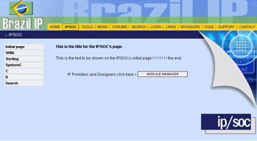
Figure 2: Brazil IP alpha version snapshots
the end of Oct. 2002. A snapshot of the site
entry page is shown in Figure 2. Similar sites have been used by IP networks in
the world such as Design-an-Reuse (http://www.design-reuse.com/). The author
will eventually donate this site to the PNM organizers, or to any institutions,
or group of people, that show enough interest/potential to implement the Brazil
IP Network.
The Brazil IP site was designed with
a number of features that are specific to support such type of a network.
The most important features are:
·
Publication
of Standards. The
site will make it public the documentation associated to the VSI/SRS standards.
These standards cover all aspects of an IC design from specification, passing
by HDL coding styles, reuse methodologies, and test/verification
techniques. The goal of that is to give
designers a world-class design methodology that will considerably improve
design practices, thus raising the quality of the final IP cores.
·
Certified
IP Repository. Once
an IP core is thoroughly validated by the ASIC Challenge it is considered
Brazil IP Certified and is deposited into the site. This will assure a quality
stamp to the core, thus establishing minimum functionality and performance
standards for potential users. The issue of assuring IP quality is fundamental
for the long-term success of this project.
·
IP
Access. A certified
IP will be owned by the IP provider that designed it, being an academic
institution or an R&D center. The fact that a core is deposited at the
Brazil IPs does not imply that all site visitors (users) will be able to
download it. Only a “one-page” description of the core will be available for
the visitors. For those interested in using the IP for academic and/or industrial
purposes a permission of the IP provider must be acquired directly from the
provider. The Brazil IP site will have mechanisms to speed up the permission
management, such that an IP provider can easily control the access to its IP
through the site. The Brazil IP in this case will only work as a broker of the
process not holding any liability for the relation provider-user. Any NDA[3]
signed between provider and user should not include Brazil IP. Given that one of the goals of the Brazil IP
Network is to expand the design activities in the country, it is expected that
academic institutions be allowed to use certified core free of charge, solely
for educational and research purposes.
·
Discussion
Forums. The Brazil
IP forum will permit its community of users to interact through a set of
on-line discussion forums. As all other services in the site, forums will be administrated and moderated
through the web.
In order to permit a fast operation, the Brazil IP site will have a
hierarchical user permission structure. This structure will allow IP providers to update their
modules and efficiently manage its relation with the user of their IP,
independent of the Brazil IP administration. The permission framework is
roughly described below.
·
Brazil
IP Administrator. The administration of the Brazil IP
site will be performed by the Brazil IP
Administrator. This user will have super-user powers in the system, being
allowed to control most functions in the site.
·
Design
Manager. Each IP
provider will be liable for its own IPs. In order to assure that, the providers will be required to register
at the Brazil IP Network through the
identification of the Design Manager (Manager) that represents it. This person
will be responsible for managing the access and status of each certified IP deposited by its institutions. The
registration of the IP Provider and its Manager will be grant by the Brazil IP
root through a system of permissions running in the site.
·
Designer.
IP Providers will
be allowed to register Designers at the Brazil IP site. A Designer will be
allowed to update only the projects they work with. To delete or add a new
project they will need the authorization of its Design Manager.
·
Visitors.
Visitors to the
site will be allowed to go around the pages, see the “one-page” description of
the IP cores, participate at the open forums, but will not be allowed to
download IPs unless authorized by the IP Provider Manager.
VIII conclusions
The work that led to this document
proved to be extremely helpful as a way of analyzing the international IP
market, and the resources available in Brazil for insertion into this market A
few conclusions can be drawn from this analysis, a follows.
The evolution of the IP market is pointing to
an increase in the demand of complete IP solutions. Thus, any new IP provider entrant, in particular those from small Brazilian DHs, should
concentrate its effort in designing cores that: (a) provide a high-valued solution
to some specific niche; (b) could eventually contribute to assemble a relevant
platform IP. Given the high costs of option (b), the new DH will have to do a
very good job in terms of identifying the right IP. This will require a very
strong support of market experts and a solid foundry partnership. It can be a
winning strategy, but it still assumes that the country has enough critical
mass in this area, and it does not have.
The PNM approach to set up local DH
is coherent. It adequately recognizes the importance of funding the DH resources for a long-term project. The creation of new financing mechanisms,
like the sector funds, could provide Brazil with enough capital to fund a few
local DHs. Nevertheless, the country
does not have enough trained designers to leverage on that. The HR mass is
scattered and urgently needs to be networked and organized around international
design standards and evaluation. In other words, the country has the capital
but not enough people to perform the task. It will be hard to set up local DHs
without first going through the experience of generating enough critical mass
in terms of design experience. Experienced designers require years of training
and (unfortunately) training new designers from scratch is not enough. They need to go through the
experience of designing and testing real-world ICs, using real-world design
methodologies for a few years. To promote that, long term funding mechanisms
like those that supported the FAPESP Genome Project, or some financial
mechanism like the Brazil IP Network accreditation by CATI/MCT will be
definitely a good strategy. This should be combined with clear design goals
toward platform IPs involving all networked institutions.
It is very important that the
microelectronics academia increase its efforts to demonstrate that: (a) it can
participate in collaborative projects;
(b) it is capable of delivering world-class R&D activities; (c) it
is capable of dealing with world-class standards and evaluation. The current
status of such community, in which separate groups make individual efforts
aiming at their own local interest, does not help anyone. On the contrary, it
only benefits the maintenance of the current situation.
As said in the introduction, this
document does not intend to be a final project. On the contrary. Its
goal is to contribute to the debate that has been undergoing in this area under
the coordination of MCT. Thus, it will serve its purpose if it can be
thoroughly scrutinized by all players in the area. Its final conclusion is that
although the DH funding strategy by PNM is going in the right direction, it is
not enough to sustain growth in the long term, without some mechanism to create
adequate design critical mass. We hope that The Brazil IP Network serves to
this purpose.
the author
Professor Guido
Araujo received his
PhD degree from
Princeton University in 1997,
under the supervision of Prof. Sharad Malik.
He is currently an associate professor at the Institute of Computing, UNICAMP, Brazil. His main research interests are in the area
of VLSI design, optimizations for
embedded processors, including
code generation and code compression
algorithms, architecture
evaluation and all aspects of
computing related to the design of
embedded systems. Professor Araujo is one of the designers of the SPAM compiler. He
was awarded a Best Paper Award at the
1996 ACM/IEEE Design Automation
Conference, and has worked as
a compiler consultant
for Conexant Systems
Inc. and Mindspeed
Technologies (USA) since 1997. He has
published scientific papers in the
ACM Trans. on Design
Automation of Electronic Systems, IEEE Trans. on
VLSI Systems, ACM/IEEE
International Symposium on Micro-architecture, ACM/IEEE Design
Automation Conference and ACM/IEEE International Symposium on Systems
Synthesis. Professor Araujo has worked as a referee for the ACM Trans. on Programming Languages and Systems, IEEE
Trans. on VLSI Systems, ACM Trans. on Design Automation
of Electronic Systems, Design Automation of
Embedded Systems and ACM/IEEE
Design Automation Conference and has served in the Program Committee of
ACM LCTES 2001. He is the
Brazilian coordinator of the
ProTeM-CC CNPq/NSF Collaborative Research Project on
Design Environments for Application-Specific Programmable Processors, a collaboration between Princeton University, MIT and UNICAMP.
bibliography
1.
IP is
a Big Business but for few Players: Analyst, by Michael Satarini, EE Times,
February 3, 2000.
2.
Foundries
Broaden their Reach with Process, IP Prowess, by David Lammers, EE Times, March
12, 1999.
3.
Productized
IP: More than Pipe Dream, by Craig Lytle, Altera Corporation, March 21, 2000.
4.
Synopsys’
Move to Free Libraires May Rattle IP Market, by Michael Santarini and Chris
Edwards, EE Times, March 20, 2000.
5.
IP Value
Depends on Other Occupants, by Mark-Eric Jones, MoSys Inc., EE Times March 21,
2000.
6.
Building
an Infrastructure for IP Reuse, by Scott Runner, Venu Sanaka and Elaine Yu,
Conexant Systems Inc., EE Times, May 15, 2000.
7.
OpenMOre
Opens More SoC IP doors, by Laura Horsey, Synopsys Inc., EE Times, May 15,
2000.
8.
Dataquest
Pegs Chip IP Market at over $400, by Peter Clarke, EE Times, May 23, 2000.
9.
Hard
IP too costly to Use Just Once, by Mahendra Jain, EE Times, January 18, 2000.
10.
Changing
Semiconductor Industry Brings Investor Opportunity, by Dan Niles, C|Net
News.context, June 27, 2000.
11.
Intellectual
Property Advisor, Gartner Dataquest, August 2000.
12.
1999
Intellectual Property Revenue by Market Segment and Function, by In-Stat MDR,
October 2000.
13.
Panel
Sees IP Role for Servide Providers, by Peter Clarke, EE Times, October 23,
2000.
14.
Dataquest
Forecasts Strident IP Market Growth, by Peter Clarke, EE Times, October 23
2000.
15.
Analysts
Seeks “Rethinking” of Semiconductor IP, by Richard Goering, EE Times, March 21,
2001.
16.
IP
Vendors making Leap from Source Code to Silicon, by Anthony Cataldo, EE Times,
May 15, 2001.
17.
Chip
IP Market Sees a Boom, by Matthew
Broersma, ZDNet, June 12, 2001.
18.
Software
Rises in Semiconductor IP Market Report, by Peter Clarke, EE Times, June 20, 2001.
19.
Software
Licenses Sees IP Market Transformation, by Peter Clarke, EE Times, August 16,
2001.
20.
The
Microelectronics National Program PNM – Design House, by Vanda Scartezini,
Informatics Policy Secretary of the Ministry of Sicence and Technology
(SEPIN/MCT), August 2001.
21.
Platform
IP for All Seasons, by Chris Edwards, EE Times, October 1, 2001.
22.
Independent
IP Providers – Design Highway to the Future, by Jerry Worchel, Cahners In-Stat
Group, November 2001.
23.
The
Market for IP-Enhanced Services, Curt Harler Inc., November 2001.
24.
IC
Design Houses: Business Infrastructure Viability, by Luiz Franca-Neto, Intel
Corporation, at the Brazilian Workshop on The Global IC Design Market, Manaus,
Brazil, November 5, 2001.
25.
Creating
Values for Partners, by Eddy Blokken, IMEC, at the Brazilian Workshop on The
Global IC Design Market, Manaus, Brazil, November 5, 2001.
26.
Reality
Hampers Vision of Interoperable IP Cores, by Junko Yoshida, EE Times, March 6,
2002.
27.
Dream
of Interoperable IP Butts up Against Reality, by Michael Santarini, EE Times
March 18, 2002.
28.
Viewpoint:
Smaller Third-party IP Vendors, by Crista Sousa, EDTN Network, April 8, 2002
29.
Semiconductor
Intellectual Property Market Raises 25%, Gartner Dataquest’s Semiconductor
Group, April 30, 2002.
30.
Research
Shows that IP Market Surged in 2001, by Ian Cameron, EE Times, May 2 2002.
31.
Virage
Logic is the Fastest Growing Semiconductor IP Company in North America, Design
and Reuse Headline News, May 8, 2002.
32.
What
are the Main Challenges to Successful IP Integration ?, by Helena Zheng, 3DSP
Corp., EE Times, May 28, 2002.
33.
Suppliers
Couple IP with Design Services to Add Value, by Michael Santarirni, EE Times,
June 11, 2002.
34.
The
Intellectual Property Business, ChipCenter News, July 10, 2002.
35.
Business
aspects of the IC design market, by Gerson Machado, INVISIX, at the Brazilian
Workshop on The Global IC Design Market, Manaus, Brazil, November 5, 2001.